|
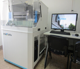
Device Name: PVA Acoustic Scanning Microscope |

|
|
Manufacturer: PVATePLa |
|
|
Function Introduction: This device is used for failure analysis of components, observing voids and defects inside chips and packages. Performance Introduction: Scanning modes: A,B,C,D,G,P,T,X,3D scanning; scanning resolution: ±0.1um; scanning range: 420×420mm; probe highest frequency: 400MHz |
|
Device Name: Electrostatic Discharge Tester |
|
|
Manufacturer:HANWA ELECTRONIC |
|
|
Function Introduction: Used for HBM/MM model ESD testing and LATCHUP latch-up testing, with a maximum of 256 PINs. Performance Introduction: PIN count: 256 PINs Maximum HBM voltage: ±8000V Maximum MM voltage: ±4000V Latch-up test voltage: 35V,1A |
|
Device Name: X-ray Fluorescence Measurement System |
|
|
Manufacturer: OXFORD |
|
|
Function Introduction: This device is used to test the thickness of component plating layers. Performance Introduction: Can simultaneously test the thickness of 4 plating layers (on substrate), resolution 1uin; spectrometer processor: 4096 channels |
|
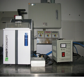
Device Name: Metal Package Device Opener |
|
|
Manufacturer: Ruifeng Xianke Technology Co., Ltd. |
|
|
Function Introduction: This device is used for opening the caps of components. Performance Introduction: Opening sample size diameter: 1mm-20mm; |
|
Device Name: ELITE ETCH ACID Opener |

|
|
Manufacturer: |
|
|
Function Introduction: This device is used for non-destructive opening and analyzing the internal damage characteristics of components. Performance Introduction: Chemical temperature range: 20℃-250℃; liquid flow rate: 1-6ml/minute; nitrogen flow rate: 2.0lpm |
|
Device Name: Stereomicroscope |
|
|
Manufacturer: HAWK |
|
|
Function Introduction: This device is used for chip inspection and 3D imaging. Performance Introduction: Maximum magnification: 200× |
|
Device Name: Optical Microscope |
|
|
Manufacturer: Olympus |
|
|
Function Introduction: This device is used for chip inspection. Performance Introduction: Features an ultra-wide field-of-view erecting eyepiece (F.N22mm), 30°, stage size 8 inches × 8 inches, travel distance 210mm × 210mm, maximum objective magnification 100× |
|
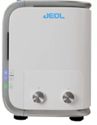
Device Name: Desktop Scanning Electron Microscope |

|
|
Manufacturer: JEOL |
|
|
Function Introduction: This device is used for failure analysis of semiconductor products at the chip level. Performance Introduction: Magnification: 10 X - 60000 X |